BiCMOS Technology Explained: The Best of Bipolar & CMOS Circuits
BiCMOS technology has revolutionised integrated circuits by blending bipolar transistors and CMOS. This innovative approach tackles the limits of traditional transistor designs. Introduced in 1983, BiCMOS marked a pivotal moment in semiconductor engineering1.
BiCMOS seamlessly merges bipolar and CMOS processes without extra fabrication steps. This efficient integration allows for shared processing techniques1. The result is integrated circuits with outstanding performance characteristics2.
One key advantage is the ability to combine analog and digital circuits on one chip. This offers designers unparalleled flexibility in creating complex electronic systems2.
BiCMOS boasts impressive speed, with switching delays as brief as 1-2 nanoseconds2. This rapid processing is vital for modern electronics requiring swift signal handling. The technology also supports high packing density, enabling powerful circuits in compact sizes2.
BiCMOS finds use in various industries, from wireless base stations to car radars1. Its balance of high performance and low power makes it ideal for today’s electronic design challenges1.
What is BiCMOS Technology?
BiCMOS technology blends bipolar and CMOS transistors in a single integrated circuit34. This innovative approach combines different transistor strengths to create more efficient electronic components.
It merges high-performance features of various transistor types. The result is versatile and potent electronic elements.
Evolution of Semiconductor Circuits
BiCMOS arose from the need to surpass traditional MOS transistor limits4. Researchers aimed to unite the best features of different semiconductor technologies.
Related Posts:


Their goal was to build a stronger solution for complex electronic systems. This led to the creation of BiCMOS technology.
- Bipolar transistors provide high-speed performance and excellent gain characteristics3
- CMOS technology offers low power consumption and high input impedance3
- BiCMOS integrates these advantages into a single circuit design4
Core Components and Structure
BiCMOS combines bipolar junction and metal-oxide-semiconductor transistors on one chip34. This allows for advanced circuit designs with multiple benefits.
Modern BiCMOS circuits can include high-quality RF inductors and capacitors3. These components are rare in standard CMOS designs.
These features make BiCMOS ideal for complex applications. Examples include analog-to-digital converters and software radio systems3.
Working Principles of Integration
BiCMOS technology enables flexible, high-performance integrated circuit designs3. It optimises circuits for specific performance needs.
Engineers use MOSFETs for high current circuits. They employ bipolar devices for specialised high-performance applications.
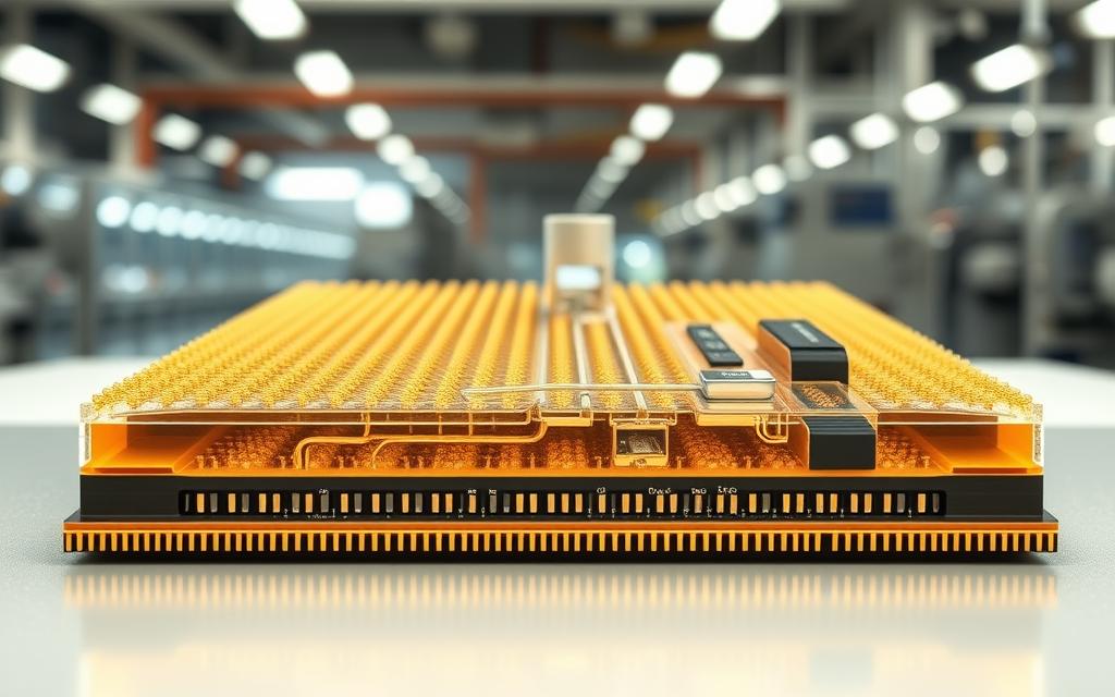
BiCMOS Fabrication Process and Architecture
BiCMOS technology creates advanced integrated circuits through sophisticated semiconductor fabrication. This process combines multiple techniques to develop high-performance electronic components. It leverages both bipolar and CMOS technologies for optimal results.
The fabrication journey starts with careful silicon substrate preparation. This forms the critical foundation for subsequent manufacturing steps in advanced semiconductor design. The substrate must meet strict specifications to ensure top-notch device performance.
Silicon Substrate Fundamentals
Preparing the silicon substrate involves several key processes:
- Selecting high-purity silicon wafers
- Cleaning and polishing the surface
- Implementing precise doping techniques
- Ensuring uniform crystal structure
Layer Deposition and Photolithography
Photolithography is crucial in semiconductor fabrication. This precise technique allows for intricate patterning of electronic components5.
SiGe BiCMOS technology enables applications beyond 50 GHz. It’s particularly useful in analog and high-speed digital systems5.
Metal Interconnect Formation
Metal interconnects link various circuit components. These sophisticated connections need careful design to reduce signal interference6.
Modern BiCMOS processes achieve remarkable performance. HBTs now demonstrate f_T values reaching 470 GHz6.
BiCMOS fabrication needs only 3-4 extra masks beyond standard CMOS techniques. This makes it efficient for creating complex integrated circuits.
Performance Advantages of BiCMOS Circuits
BiCMOS technology is a game-changer in integrated circuit design. It offers outstanding performance advantages over traditional semiconductor technologies7. These circuits blend CMOS and bipolar transistors, delivering top-notch electrical performance8.

- Enhanced current driving capability that allows efficient load management7
- Superior switching speeds compared to conventional CMOS designs8
- Exceptional noise immunity across various operating conditions
- Low power consumption while maintaining high-performance characteristics7
BiCMOS technology excels in handling complex electronic needs. It operates at impressive speeds, with logic circuits achieving remarkable performance metrics.
BiCMOS logic circuits can work twice as fast as standard CMOS circuits at 1.5V supply voltage8.
The true strength of BiCMOS lies in its ability to bridge analog and digital domains seamlessly.
BiCMOS efficiently drives high-capacitance loads, making it perfect for input/output intensive applications7. Its integrated design reduces external component needs.
This optimises overall power consumption and system performance. BiCMOS truly stands out in the world of integrated circuits.
Applications in Modern Electronics
BiCMOS technology has transformed modern electronic devices. It bridges analog and digital signal processing. Mixed-signal ICs enable sophisticated functionality through advanced semiconductor integration.
Mixed-Signal Integration
BiCMOS technology combines analog and digital circuits seamlessly. This integration creates compact and efficient electronic systems9.
Flexible transistor architectures allow precise signal management. They offer remarkable performance characteristics9:
- Field-effect mobility for NMOS: 160 cm²/V·s
- Field-effect mobility for PMOS: 34 cm²/V·s
- Threshold voltage for NMOS: 0.95 V
- Threshold voltage for PMOS: -1.9 V
RF and Communication Systems
BiCMOS innovations greatly benefit wireless technology. RF circuits use these advanced platforms to boost communication system performance10.
European BiCMOS platforms now tackle submillimeter-wave and THz applications. Power measurements extend up to 190 GHz10.
High-Performance Computing
High-speed computing requires sophisticated semiconductor technologies. BiCMOS enables rapid data processing through advanced transistor configurations.
STMicroelectronics’ 55-nm BiCMOS platform shows impressive capabilities. It achieves fT values of 320 GHz and fMAX of 370 GHz10.
BiCMOS technology’s flexibility ensures its ongoing relevance. It continues to develop sophisticated electronic systems across various technological frontiers.
Challenges and Limitations in BiCMOS Implementation
BiCMOS technology poses significant fabrication challenges for semiconductor manufacturers. The integration of bipolar and CMOS transistors requires sophisticated processes, introducing technical hurdles11. This complexity may reduce manufacturing yield due to potential emitter-collector shorts11.
Thermal management is a critical limitation in BiCMOS circuits. Devices face reliability issues when junction temperatures exceed 150°C, potentially increasing failure rates by 50%12. The intricate integration creates thermal stress points that need careful management.
Cost considerations significantly impact BiCMOS implementation. Fabrication can increase production expenses by 10-15% due to complex manufacturing processes12. Scaling challenges further complicate matters, making it difficult to maintain performance across different transistor types.
Ongoing research aims to address these limitations. Scientists explore innovative techniques to improve fabrication, thermal performance, and reduce production costs. Despite challenges, BiCMOS technology remains crucial for advanced microelectronics12.
FAQ
What is BiCMOS technology?
How does BiCMOS differ from traditional CMOS or bipolar technologies?
What are the primary applications of BiCMOS technology?
What are the key manufacturing challenges of BiCMOS?
Why is BiCMOS considered superior to single-technology approaches?
How does BiCMOS handle mixed-signal integration?
What are the future prospects for BiCMOS technology?
Source Links
- https://anysilicon.com/bicmos/
- https://www.tutorialspoint.com/bicmos-technology-fabrication-process-and-applications
- https://en.wikipedia.org/wiki/BiCMOS
- https://www.elprocus.com/bicmos-technology-fabrication-and-applications/
- https://www.eecg.utoronto.ca/~tcc/bctm_06_sv.pdf
- https://www.ihp-microelectronics.com/php_scripts/publications/manuscript_files/ruecker-ruecker-bcicts-2019_accepted-2021.pdf
- https://www.westfloridacomponents.com/blog/what-is-bicmos-technology/
- https://www.academia.edu/66652770/Optimization_of_digital_BiCMOS_circuits_an_overview
- https://www.nature.com/articles/s41528-017-0001-1
- https://www.ihp-microelectronics.com/php_scripts/publications/full_text_final_files/karakuzulu-zimmer-j-of-microw-1-288-2021-2021.pdf
- https://link.springer.com/chapter/10.1007/978-1-4615-3208-8_7
- https://www.cambridge.org/core/books/reconfigurable-circuits-and-technologies-for-smart-millimeterwave-systems/cmos-and-bicmos-technologies/9EDACB658480027C11785D813468A65E